Vertical power devices
Ga₂O₃ SBDs and normally-off vertical MOSFETs that combine multi-kilovolt blocking, low conduction loss, and compact chip area.
 Extreme Power & Integrated Devices Laboratory
Research 02 · Extreme & power electronics
EPID translates ultra-wide bandgap materials into vertical switches and sensors that control high voltage, resolve invisible radiation, and remain dependable where heat, electric field, and energetic particles challenge ordinary electronics.
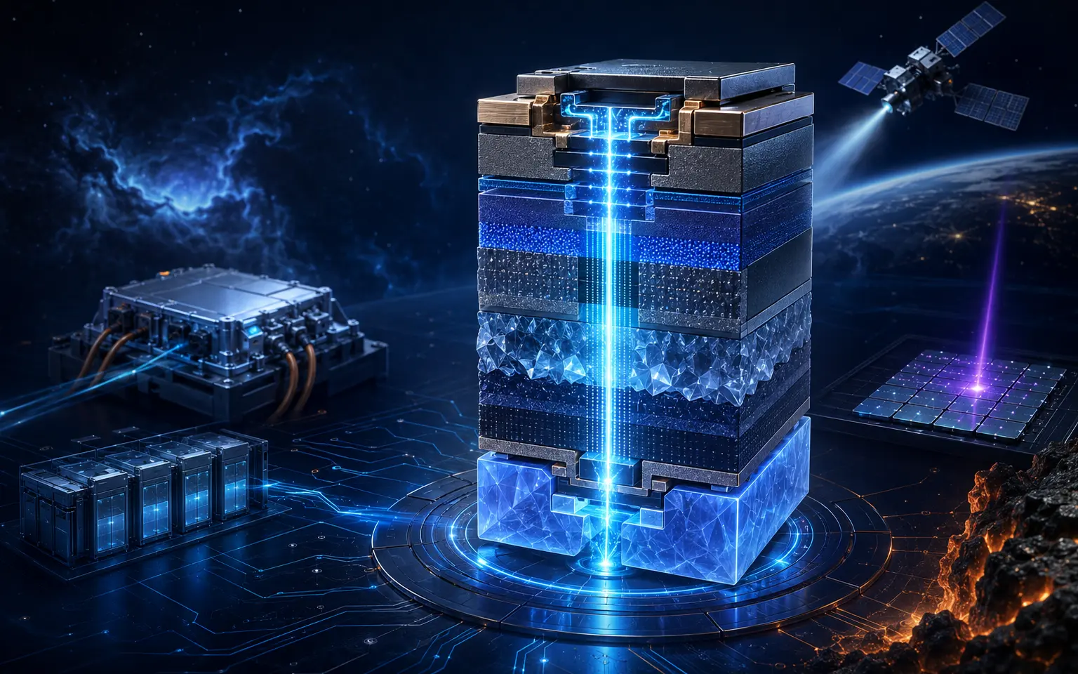
Overview
We co-design device geometry, interfaces, thermal pathways, and reliability so that material advantages become measurable system-level performance.
Ga₂O₃ SBDs and normally-off vertical MOSFETs that combine multi-kilovolt blocking, low conduction loss, and compact chip area.
Solar-blind DUV and direct X-ray imagers designed for weak signals, low standby power, high temperature, and harsh operating conditions.
Materials, devices, and circuits engineered against total ionizing dose, displacement damage, and destructive single-event effects in space.
Device architecture
Vertical conduction uses the chip thickness for voltage blocking and the device area for current, enabling compact high-power rectifiers and switches.
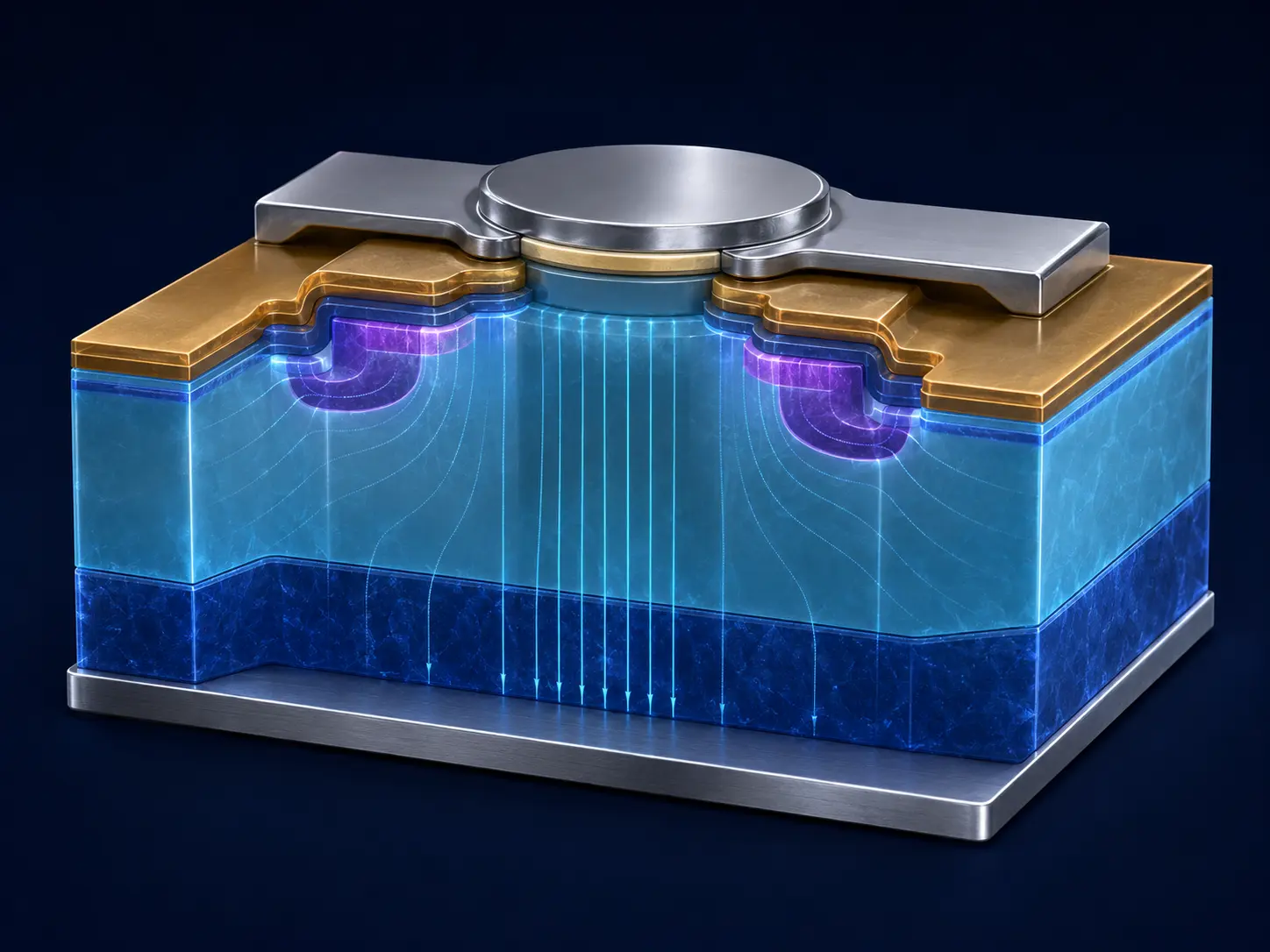
Field plate and mesa termination spread the surface field while N-implanted rings suppress the anode-edge field peak.
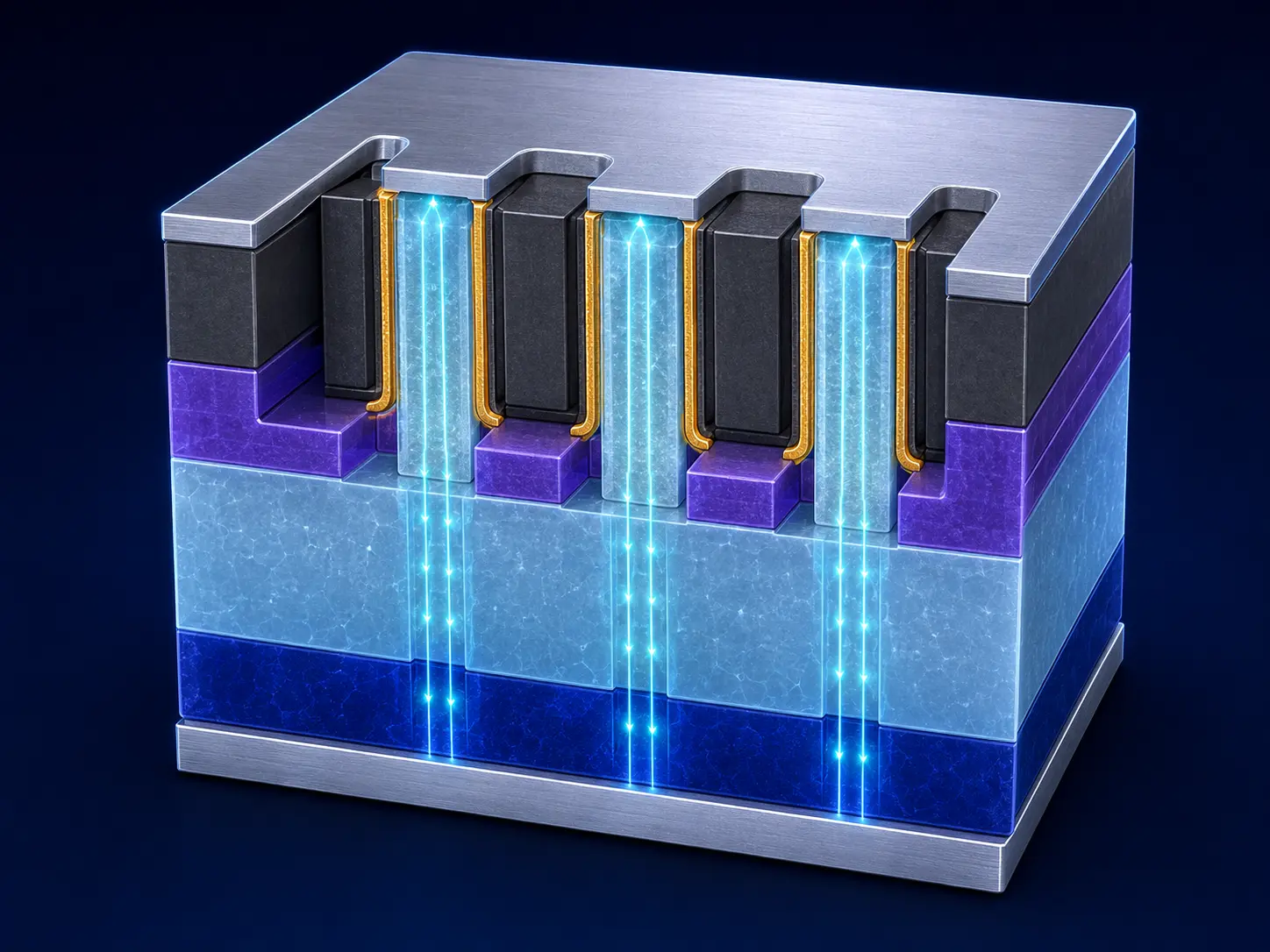
ALD Al₂O₃ wraps each fin as the gate dielectric; narrow fins deplete at zero bias, while N-implanted CBL regions confine the vertical current path.
Thickness and net donor density set the blocking-voltage and on-resistance trade-off.
Field plates, junction terminations, trenches, and guard structures move peak field away from vulnerable edges.
Contact barriers, gate dielectrics, and interface traps govern leakage, threshold stability, and dynamic loss.
Substrate thinning, backside contacts, heat spreaders, and heterogeneous integration address Ga₂O₃'s low thermal conductivity.
Vertical rectifier
Low-loss unipolar rectification with multi-kilovolt blocking and robust surge capability
Vertical switch
Normally-off electrostatic control for safe, fast, and efficient high-voltage switching
2025–2026 direction
The frontier is shifting from isolated breakdown demonstrations to manufacturable architectures with current capability, switching stability, and mission-level reliability.
High-k bilayer field plates, implanted protection rings, JTE, and trench RESURF suppress premature breakdown.
Sub-micron fin depletion enables enhancement-mode switching without a native p-type Ga₂O₃ body.
Surface preparation, anisotropic contacts, and heterojunctions balance turn-on voltage, leakage, and stability.
Surge, forward-bias degradation, high temperature, and single-event burnout are designed into the device from the start.
Extreme-environmental devices
UWBG devices combine low intrinsic carrier density, high breakdown field, and radiation response for imaging and electronics beyond conventional environments.
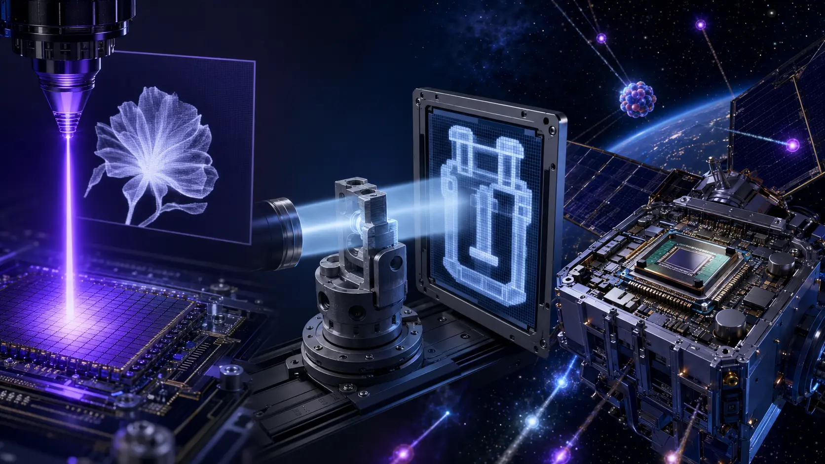
Solar-blind imaging
β- and α-Ga₂O₃ photodiodes, phototransistors, and detector arrays for sub-280 nm imaging with ultra-low dark current and strong visible-light rejection.
Direct conversion
High-density Ga₂O₃ crystals and epitaxial films convert X-ray photons directly into charge for low-dose dosimetry and pixelated radiographic imaging.
Space electronics
Power switches and sensors are evaluated under protons, neutrons, heavy ions, electrons, and ionizing radiation to reveal failure physics and harden operation.
Reliability platform
We reproduce electrical, thermal, optical, and radiation stress; locate the physical failure path; and return the learning to materials and device design.
High-field blocking, surge current, repetitive switching, bias-temperature stress
Self-heating, extreme temperature, thermal cycling, interface resistance
Protons, neutrons, heavy ions, electrons, X-rays, and gamma rays
DLTS, low-frequency noise, emission microscopy, TEM, TCAD, and particle transport
Join EPID
We welcome students and researchers interested in vertical power devices, DUV and X-ray imaging, radiation effects, reliability physics, and extreme electronics.
Contact EPID ↗