Crystal & phase engineering
Stabilizing α, β, and ε(κ) phases through substrate selection, surface chemistry, temperature, and precursor design.
 Extreme Power & Integrated Devices Laboratory
Research 01 · Ultra-wide bandgap semiconductors
EPID studies Ga₂O₃ as a complete materials platform—from precursor chemistry and polymorph selection to defects, interfaces, and transferable epitaxial layers. Our goal is to create the materials foundation for electronics that operate beyond today's voltage, temperature, and efficiency limits.

Overview
We connect crystal chemistry, epitaxial growth, structural characterization, and defect physics. Each result informs the next growth cycle, moving Ga₂O₃ toward controllable, reproducible, and device-ready material.
Stabilizing α, β, and ε(κ) phases through substrate selection, surface chemistry, temperature, and precursor design.
Controlling nucleation, orientation, thickness, alloy composition, and donor incorporation using MIST-CVD and MOCVD.
Linking extended and point defects to transport, breakdown, trapping, and long-term device reliability.
Epitaxy
Complementary reactors let us explore chemistry rapidly, then translate the learning into uniform and scalable epitaxial layers.
Polymorphs
The properties of Ga₂O₃ depend strongly on its atomic arrangement. We compare growth windows, phase stability, strain, polarity, and defect formation across the three polymorph families most relevant to epitaxial electronics.
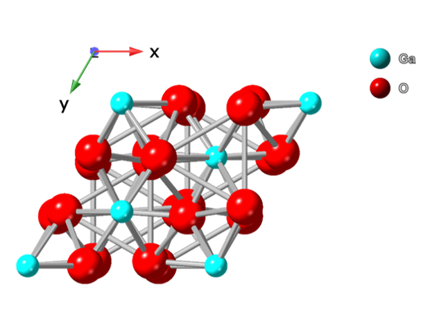
Corundum · metastable
Heteroepitaxy on c-plane sapphire, phase-pure growth windows, donor incorporation, and strain-aware defect control using MIST-CVD.
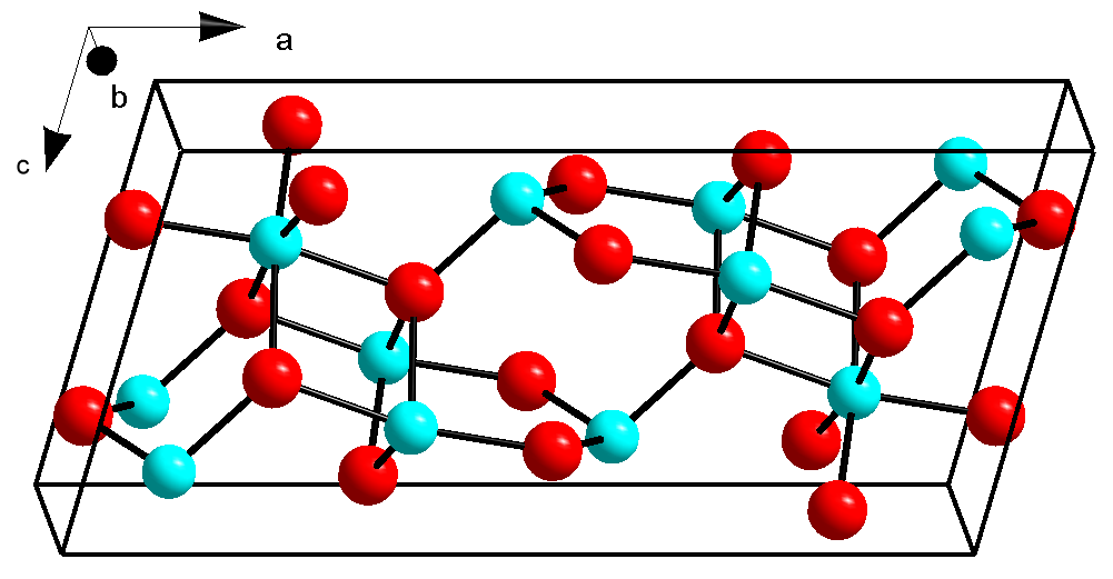
Monoclinic · stable
Homo- and heteroepitaxial films, alloy and doping control, vertical device layers, and interface engineering for high-field power electronics.
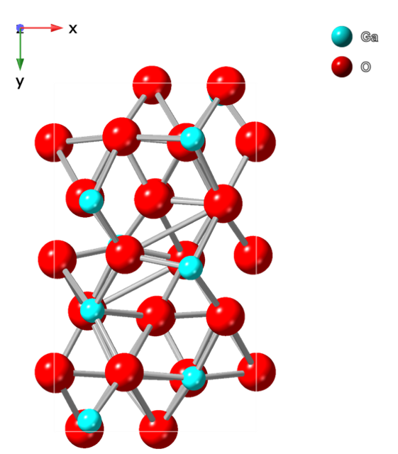
Polar orthorhombic · metastable
Phase stabilization, rotational-domain suppression, polarization-enabled heterostructures, and thin-film growth on crystalline templates.
Defects & analysis
Atomic-scale images reveal where an epitaxial layer begins, how lattice mismatch is accommodated, and which defects propagate into the active material. We connect these observations to growth conditions and electrical behavior.
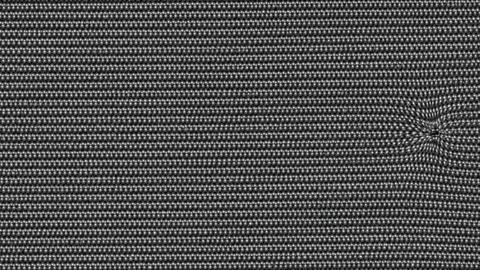
Phase, orientation, strain, mosaicity, and epitaxial relationship
Nucleation, step evolution, roughness, and surface morphology
Interfaces, dislocations, stacking faults, domains, and chemistry
Chemical states, optical centers, and electrically active traps
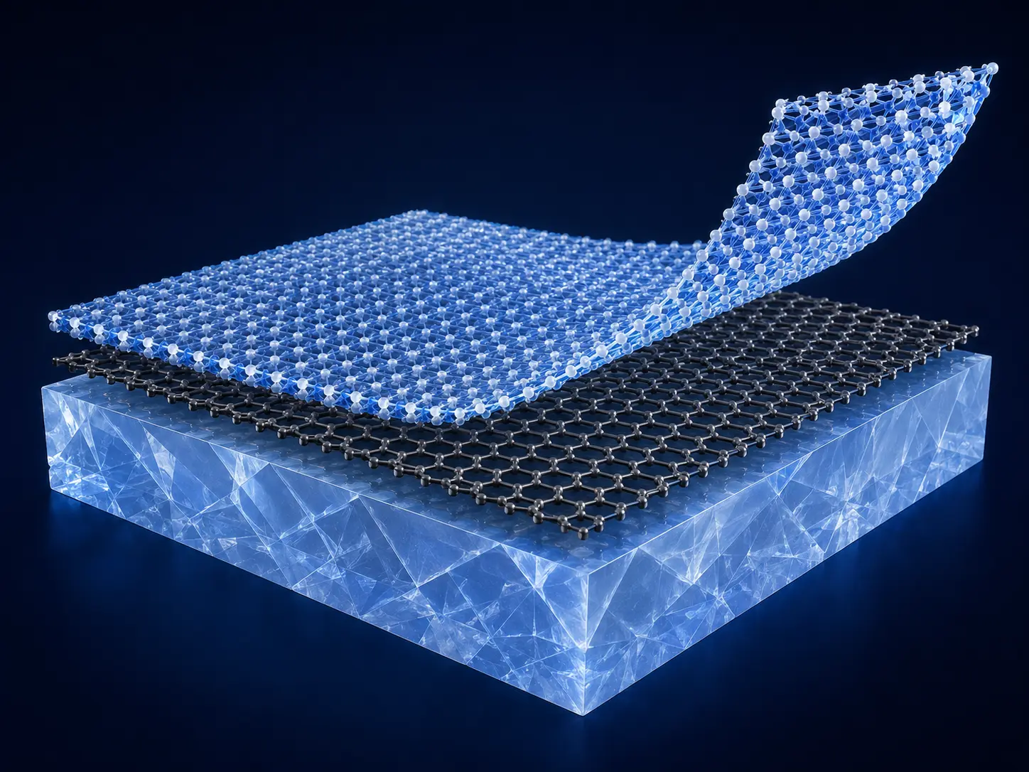
Future platform · Remote epitaxy
We explore remote epitaxy through atomically thin 2D interlayers. The approach aims to preserve crystallographic guidance during growth while weakening interfacial bonding—opening paths to freestanding Ga₂O₃ membranes, heterogeneous integration, and reusable crystalline substrates.
Join EPID
We welcome students and researchers interested in Ga₂O₃ epitaxy, advanced characterization, defect physics, and power devices.
Contact EPID ↗